Laser Marking System
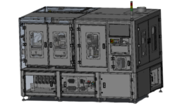
This equipment is for laser marking for the substrate.
The equipment features have a nanosecond UV laser source and i3 engineering marking optics in the device, which can be processing the semiconductor substrate products.
- The Max. loading Strip size is 510mm X 510mm
- The Max. loading Strip thickness is 2.0mm
- The laser marking is available to 2D matrix Dara, QR code, and bar code with alphabet and numbers
- The laser marking material is available for Copperplate, PCB surface, lead-frame, and others
This system will utilize the i3 engineering technology and can support the base on customer required